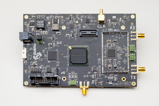
It would take little effort on the part of a user with no soldering experience to attach a connector; I am interested to know if that area will assist with 4x4 MIMO, or if it is available if one wishes to have another antenna. I notice that the top-center contact appears to have a pathway to the FPGA, though that might mean nothing. I admit that I haven't take more than a glance at the board specifications, and my question(s) may be answered there.
Are there any pictures available of the GPIO and down-converter daughter-boards? I'm planning to get some enclosures cut, and I want to get some enclosures cut for the daughterboards, or get an enclosure build to house at least one bladeRF, GPIO expansion board, and two to three RF band-expansion boards. I will put a post up when I get my final layout finished, if anyone wishes to order enclosures with me, or buy some from me when I get them made.
Feel free to PM me, or email me at [email protected] or [email protected], if you're interested in getting an enclosure produced for our bladeRFs.
By the way, to the creators of the bladeRF: This is a great board.